

Technical Services
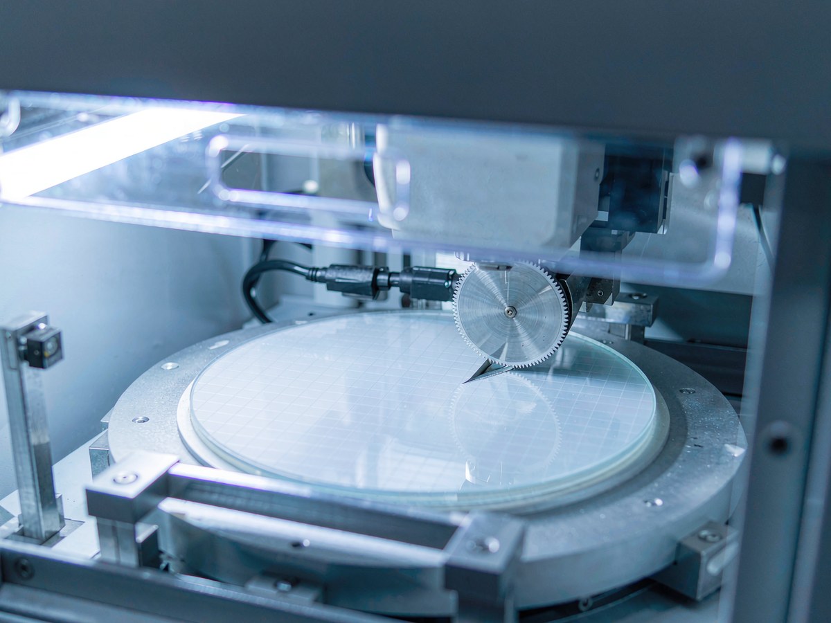
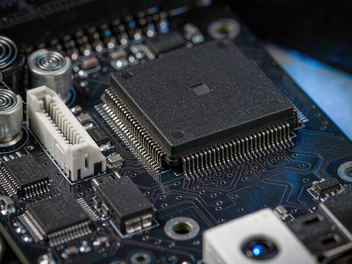
Hypersemi (Zhuhai Hypersemi Co., Ltd.) is a power semiconductor manufacturer (IGBT, SiC, MOSFET, modules and discretes) offering three professional service lines to customers worldwide: custom chip design, chip failure analysis, and wafer processing (CP test · wafer thinning · wafer dicing · IC programming). Backed by advanced equipment, a senior engineering team and standardized processes, we deliver one-stop support — from design and analysis to processing — for design houses, IDMs and end manufacturers.
Design Services
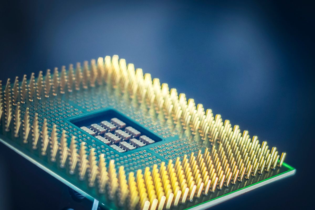
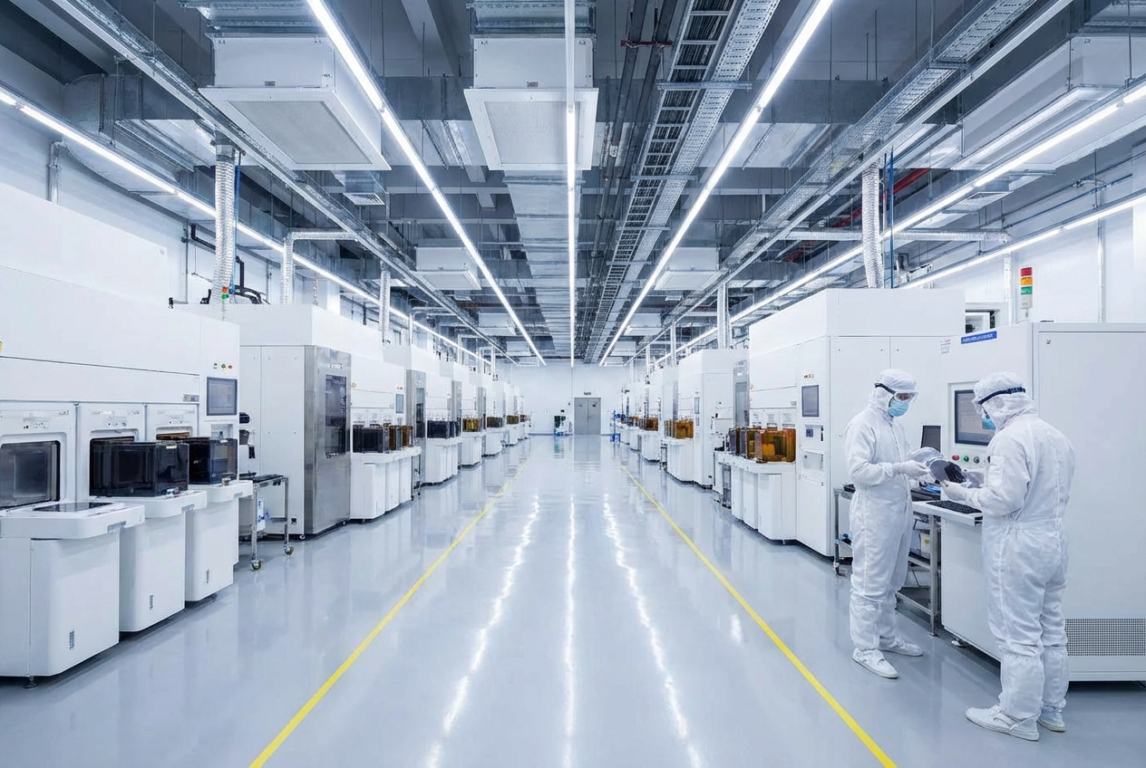
Two capability lines: custom chip design and failure analysis.
Processing Services
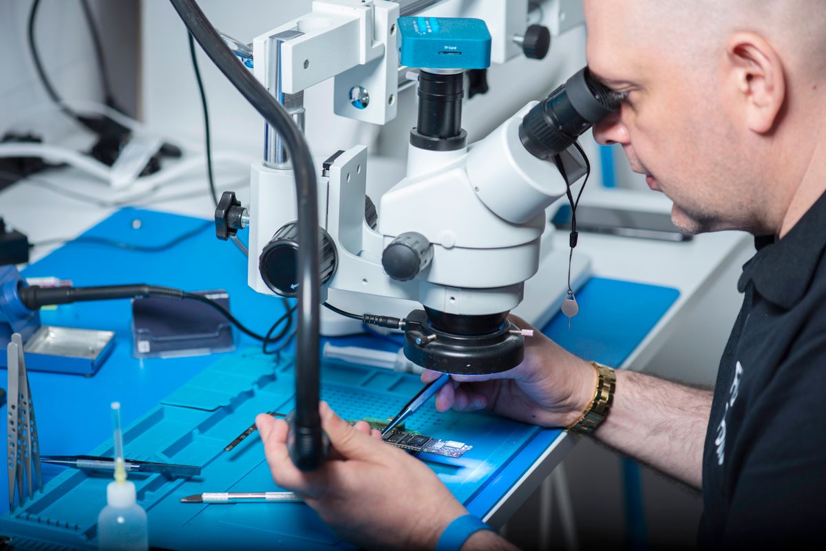
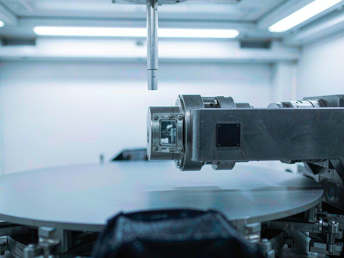
Wafer processing: CP test · thinning · dicing · programming.
Get Tech Support
Tell us what you need — our engineering team will get back to you shortly.
Contact usHow we work
-
01
Requirement review
Share your specs, volumes and application — our engineers review feasibility and the best route.
-
02
Proposal & quote
Across chip design, failure analysis and wafer processing, we propose the right solution and terms.
-
03
Execution & verification
Standardized workflows keep you updated with data at key milestones.
-
04
Delivery & support
On-time delivery of reports or devices, with ongoing engineering support.